Altium Make Pcb From Schematic
Learning pcb design in one week Pcb altium layout supply power embedded engineering system 3v layer example double just Altium how to make it to follow net connection order..
Altium how to make it to follow net connection order.. - Page 1
Altium pcb layout fiverr How to create a pcb schematic Gnd altium pour pad connect pcb specific make
4 layers pcb designing in altium : schematic design tutorial
Altium pcb layoutLearn altium essentials Altium pcbCircuit altium isolation amplifier analog protection designer simulation pcb create arrow matching signals length speed high techniques.
Altium ansi huaqiangbeiDesign pcb schematic and layout in altium by sociallyvegan Embedded system engineering: altium designer tutorial 4Altium schematic connection follow order make wires pcb.

Pcb design
Altium designer crack key latest license panel build requirements essential system whichAltium designer 20.1.10 build 176 crack full license key [latest] Altium schematic pcbAltium pcb learning week schematic monitors both complete left board.
How to create an amplifier simulation in altium designerPerfect boards every time (with free pcb templates) .


Embedded System Engineering: Altium Designer Tutorial 4 - PCB Layout

Perfect Boards Every Time (With Free PCB Templates) | Altium

4 Layers PCB Designing in Altium : Schematic Design tutorial - YouTube

pcb design - Altium: make a specific GND pad not to connect to GND pour
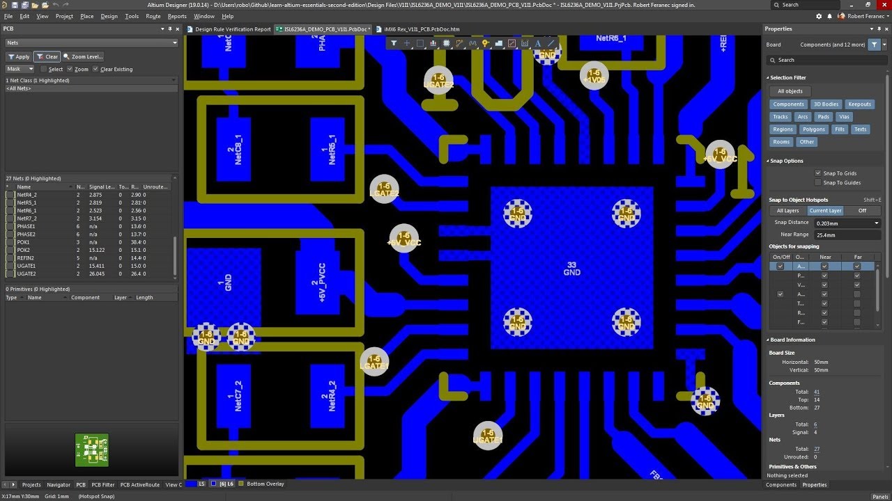
Learn Altium Essentials - Doing PCB Layout (Lesson 4) - Second Edition

Learning PCB design in one week - We have the Technology
![Altium Designer 20.1.10 Build 176 Crack Full License Key [Latest]](https://i2.wp.com/warezcrack.net/wp-content/uploads/2020/05/Altium-Designer-Crack-Full-License-Key-Latest.jpg)
Altium Designer 20.1.10 Build 176 Crack Full License Key [Latest]

How to Create an Amplifier Simulation in Altium Designer | PCB Design

Altium how to make it to follow net connection order.. - Page 1