Altium Find Net In Schematic
How to highlight nets to simplify schematics & pcb designs Altium designer in a minute: how to find all schematic nets Embedded system engineering: altium designer tutorial 4
Altium Schematic Preview | Details | Hackaday.io
Altium designer [schematic»set net colors] Altium designer embedded engineering system dialog shown browse button library choose will Altium nets command highlighting objects similar using find after
Altium schematic designer nets highlight example highlighting pcb simplify highlighted without
Altium schematic connection follow order make wires pcbAltium basic schematic development Altium: "net [] contains floating input pins", but they seem to beAltium trace designer spacing minimum identifying nets selecting class pcb width using.
Altium : learn altium essentials doing pcb layout lesson 4 secondHow to trace a net in altium designer viewer (search for all places a Kicad altium hackaday converterShow components in altium schematic, but exclude from design.

Altium designer getting started user guide & video tutorials
Altium colors schematic designer setAltium schematic Working between the schematic and the boardAltium has its 2kicad moment.
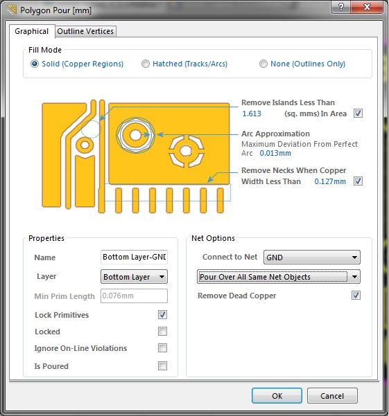
Embedded system engineering: altium designer tutorial 3Identifying minimum pcb trace spacing and width in altium designer Altium polygon layer select embedded engineering system place properties want whereAltium designer schematic.

Altium how to make it to follow net connection order..
Altium schematic input seem floating connected contains pins they but errors parent connect even its ifAltium schematic hackaday io amplifier Altium schematic previewAltium schematic components exclude show but.
Altium pcb documentation routing vault migrated supported concordAltium hierarchical schematics duplicate Altium search signal viewer trace designer places used awkward though pretty.

How to trace a net in Altium Designer viewer (search for all places a

schematics - Altium: Duplicate NET in hierarchical design - Electrical

How to Highlight Nets to Simplify Schematics & PCB Designs | PCB Design
![Altium: "Net [] contains floating input pins", but they seem to be](https://i2.wp.com/i.stack.imgur.com/65iB4.png)
Altium: "Net [] contains floating input pins", but they seem to be
Embedded System Engineering: Altium Designer Tutorial 4 - PCB Layout
![Altium Designer [Schematic»Set Net Colors] - YouTube](https://i.ytimg.com/vi/QNuYXhN2BNM/maxresdefault.jpg)
Altium Designer [Schematic»Set Net Colors] - YouTube

Working Between the Schematic and the Board | Altium Designer 17.1 User

Altium Basic Schematic Development - YouTube
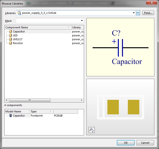
Embedded System Engineering: Altium Designer Tutorial 3 - Circuit Schematic